A Digital Vacuum Tube Analyzer and Curve Tracer
Part Two: How it Works
Note: This article describes a project that I built for myself. It is not a product that I am manufacturing or offering for sale. For various reasons, I am not releasing the schematics, PCB layouts, firmware, or software used in this project.
This is the second of two articles. Part one describes the features of the tube analyzer. Part two (this article) discusses its design and implementation.
Overview of the Hardware
The block diagram below shows the overall structure of the tube analyzer hardware. The device contains five specialized power supplies for applying voltages and measuring currents in the tube under test: two high-voltage positive supplies, two low-voltage negative supplies, and a heater supply. An I2C bus connects all of the power supplies to a master controller which coordinates their operation. The I2C bus is a simple bidirectional two-wire bus that transmits commands from the controller to the power supplies, and carries results (e.g., current readings) back from the power supplies to the controller. The use of the I2C bus permits a modular design. Each power supply is independent of the others, and additional supplies could be added without changing the existing hardware.

The host PC communicates with the tube analyzer via a standard USB interface. A USB-to-serial converter chip in the tube analyzer causes the device to appear as a standard RS-232-style serial port to the PC. The serial transmit and receive signals then connect to the master controller via a pair of opto-isolators.
There are therefore two protocol conversions between the PC and the tube analyzer power supplies: first from USB to serial transmit and receive, and then from serial to I2C. This may seem unnecessarily convoluted, but it has two big advantages over a more direct conversion from USB to I2C. The first advantage is that every major operating system contains drivers for serial ports. By making the device appear as a serial port, it is easier to make the PC software portable across operating systems. And in fact, I have successfully tested the device and its software on MacOS, Windows, and Unix/Linux computers. The second advantage is that the serial transmit and receive signals are unidirectional and can easily be sent through opto-isolators. The opto-isolators eliminate any chance that a hardware malfunction could send high voltages into the user's PC. Everything beyond the opto-isolators is completely isolated electrically from the PC. Even the grounds are separate.
The controller and all of the power supplies are implemented with various flavors of PIC microcontrollers—six PIC chips altogether. Each PIC chip is a self-contained 8-bit computer with flash memory and RAM. In addition, the PIC chips have various combinations of digital and analog peripherals built into them. The peripherals include operational amplifiers, analog-to-digital converters (ADCs), digital-to-analog converters (DACs), pulse width modulators (PWMs), timers, and serial and I2C interfaces. PIC chips are available in dual inline packages (DIP), which makes them easy to use in breadboards. A pretty decent free C compiler is available for programming them.
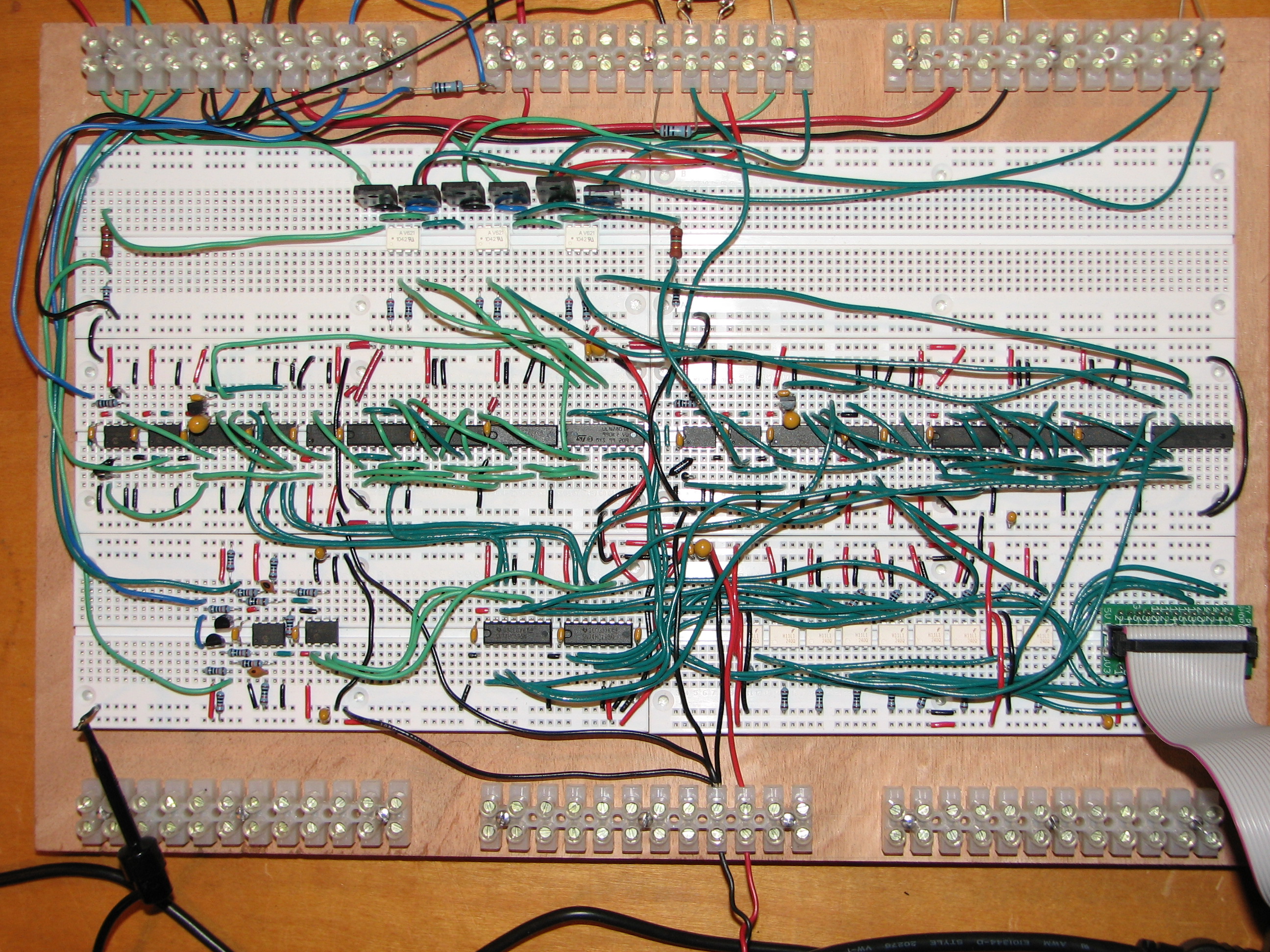
Using the PIC chips greatly simplified the hardware. At right is a photo of an early prototype that I built using discrete DACs, ADCs, and op amps. Nearly all of the circuitry in the photo was later replaced by six PIC chips.
High-Voltage Power Supplies
Supplying the desired voltages to the plates and screens of tubes presented several challenges. The goal was to be able to provide any voltage from 0 to 500 volts at a current of up to 500 mA. But 500 V × 500 mA is 250 watts—a lot of power. Implementing two such power supplies in the conventional way would require one or two very substantial power transformers.
Another problem stemmed from the need to measure the current flowing into each electrode. The way to measure current with a microprocessor is by measuring the voltage drop produced by the current flowing through a small sense resistor. For example, a 1-ohm sense resistor generates 1 mV of voltage for every 1 mA of current. The obvious place to put the sense resistor would be in the positive power supply line. But that is not a convenient place for measuring the voltage drop, because both sides of the resistor are at very high potentials. Microprocessor ADCs are designed to measure small voltages relative to ground. They can't measure a small voltage drop across a resistor floating at several hundred volts above ground.
If the current sense resistor were instead inserted in the ground leg of the power supply, the sense voltage would then be small relative to ground potential. (It would be negative, but at least it would be small.) But that means the two high-voltage supplies could not share a common ground. They would need separate power transformers, or at least separate windings on a shared power transformer.

There is a tricky solution to these problems, and although I came up with it independently, I have no doubt it has been used many times in the past. It relies on the fact that we can take a measurement very quickly, so the voltages only need to be applied to the tube for a brief time. The idea is shown in the simplified diagram at right. (Note: the switches in the diagram are in reality power MOSFETs controlled by the PIC microprocessor.) The key element is the capacitor in the center of the diagram. It is a very large capacitor. We charge the capacitor to the desired voltage, connect it to the tube by closing the "Measure" switch, and quickly take our measurement. If we are quick enough and the capacitor is large enough, its voltage will sag only a negligible amount during the measurement. In effect, the large capacitor is our power supply.
The "Charge" and "Discharge" switches (again, they are actually MOSFETs) are used for charging the capacitor to the desired voltage prior to the measurement. Using the voltage sense ADC, the PIC chip constantly monitors the voltage on the capacitor. If it is too low, the PIC closes the "Charge" switch and starts charging the capacitor. If the voltage is too high, it instead closes the "Discharge" switch to discharge the capacitor. When the voltage is just right, both switches are left open. To take a measurement, the capacitors in both high-voltage supplies are brought to their desired levels in this way. Then both "Measure" switches are closed, the measurement is quickly taken, and the "Measure" switches are opened again.
There is a small current sense resistor Rsense in the ground leg of the capacitor. When current flows into the tube, the ungrounded end of Rsense develops a small negative voltage. This is inverted and amplified by an op amp (not shown) and then measured by the current sense ADC.
How much does the capacitor voltage sag during a measurement? Not much. I used 500 µF capacitors, and the maximum current we aim to handle is 500 mA. This gives a maximum sag rate of 1 volt per millisecond. Since measurements are much faster than a millisecond, the voltage sags by much less than a volt. That is more than precise enough for the high-voltage supplies. And since we are constantly monitoring the voltage via the voltage sense ADC, we always know what the actual voltage was during a measurement, even if it was not exactly what we asked for. When plotting plate curves, for example, it doesn't matter if we requested 250 volts and only got 249.5 volts. The voltage sense ADC will report the actual voltage, and we can plot the point exactly where it belongs on the graph.
This approach has worked out very well in practice, and it has some big advantages. Since the B+ supply is used only for charging capacitors, it does not need to be particularly powerful. The same B+ supply can be used for multiple high-voltage supplies. A shorted tube causes high currents, but those high currents quickly drain the capacitor, limiting the amount of energy that can be dumped into the tube. (In practice, protection circuitry detects the overload condition and aborts the measurement immediately.)
I should emphasize that the diagram above is simplified. In reality, the current sense circuit has two ranges so that it can capture accurate measurements for both small preamp tubes and large power tubes. And there is some additional protection circuitry to keep the tube analyzer from being damaged by shorted tubes.
Low-Voltage Power Supplies
Compared to the high-voltage supplies, the low-voltage supplies are simple and straightforward. This is because their requirements are less demanding. They do not need to deliver much power at all, and they have no provision for measuring current. They do, however, need to be more precise than the high-voltage supplies, because control grids are more sensitive than anodes and screen grids.

The simplified diagram at right shows the overall design of the low-voltage supplies. Essentially, each supply is made up of a DAC and an amplifier with a high-voltage output stage. The amplifier is a standard op amp inverting amplifier, except that the op amp is augmented with a one-transistor output stage that can handle the required voltages. The transistor is in the feedback loop of the amplifier, so the output voltage is very precisely controlled by the setting of the DAC.
You may be surprised to see that the feedback goes to the positive input of the op amp. That is because the output transistor is an inverting stage. I.e., when the output of the op amp goes more positive, the output of the transistor goes more negative. Because of this, the roles of the positive and negative op amp inputs are reversed.
The circuit shown is a simplified version that, in practice, oscillates. The output transistor adds quite a bit of gain in the feedback loop—more gain than the op amp's internal frequency compensation is designed to handle. To prevent oscillation, I had to add some additional compensation. Also, the actual implementation has some components which protect the circuit from shorted tubes.
I originally planned to lay out a low-voltage supply PCB and then build two of them. However, the circuit turned out to be so simple that both supplies fit easily on the 3.8" × 2.5" PCBs that I used.
In the future I want to redesign the low-voltage supplies so that they can drive the grids far into the positive voltage region and measure the currents flowing into the grids. Once the design is finished and the new low-voltage supply PCBs are built, I'll be able to swap them in without any changes to the rest of the hardware.
Heater Power Supply

The heater supply is a conventional buck-mode switching supply. A pulse width modulator (PWM) in the PIC chip turns a MOSFET switch on and off at a rapid rate. The resulting pulses of variable duty cycle are smoothed by a filter made up of an inductor and a capacitor. A Schottky diode provides a return path for the inductor current during the "off" portions of the cycle.
Not shown in the simplified diagram at right are the regulator components. The voltage is sensed at the output by an ADC in the PIC chip. The current is also sensed at the output by an INA250A3 current monitor chip and an ADC in the PIC chip. The INA250A3 is designed to be placed in the positive leg of the output at voltages up to 36V, which is more than adequate for this application.
The firmware in the PIC chip continuously monitors
the output voltage and current. It compares the output voltage
with the set point and adjusts the duty cycle of the PWM
accordingly. Switching power supply controllers use a variety
of methods for adjusting the PWM.
A flexible approach uses a
proportional-integral-differential (PID) controller.
A PID
controller starts with an error value which is simply the
difference between the measured output voltage and the desired
voltage.
 The error is positive if the voltage is too high, or
negative if it is too low. The PID controller adjusts the PWM
duty cycle based on the error itself (proportional control),
the accumulated error over time (integral control), and the
rate of change of the error (differential control). The
PIC16F1615 chip that I used for this application has a built-in
math accelerator designed for these calculations. I used it,
but set its parameters to do simple integral control only.
Integral control is well-suited to this application because it
ramps up the output voltage slowly rather than hitting the tube
with the full voltage all at once. It is stable and very precise,
but it does not respond quickly to changes in the load. That doesn't
matter here, since a tube heater is a very stable load.
The error is positive if the voltage is too high, or
negative if it is too low. The PID controller adjusts the PWM
duty cycle based on the error itself (proportional control),
the accumulated error over time (integral control), and the
rate of change of the error (differential control). The
PIC16F1615 chip that I used for this application has a built-in
math accelerator designed for these calculations. I used it,
but set its parameters to do simple integral control only.
Integral control is well-suited to this application because it
ramps up the output voltage slowly rather than hitting the tube
with the full voltage all at once. It is stable and very precise,
but it does not respond quickly to changes in the load. That doesn't
matter here, since a tube heater is a very stable load.
Under normal steady-state conditions, the regulator firmware ignores the output current. But whenever the current goes above the design limit of 3.2 amps, the firmware alters the error signal to make the PID controller believe that the output voltage is too high. This very effectively limits the output current to a safe value, which protects the circuitry from the current surge that would otherwise occur when powering up a cold heater. It also protects against shorted heaters. To test the current limiting, I wrote a small program that plots the heater voltage and current vs. time. At left is the plot for a 6AS7GA tube, which has a 6.3 volt heater that nominally draws 2.5 amps. In the plot you can see the current limiting in effect for the first 11 seconds, after which the tube's heater has warmed up enough that its current is below the limit of the supply.
Construction
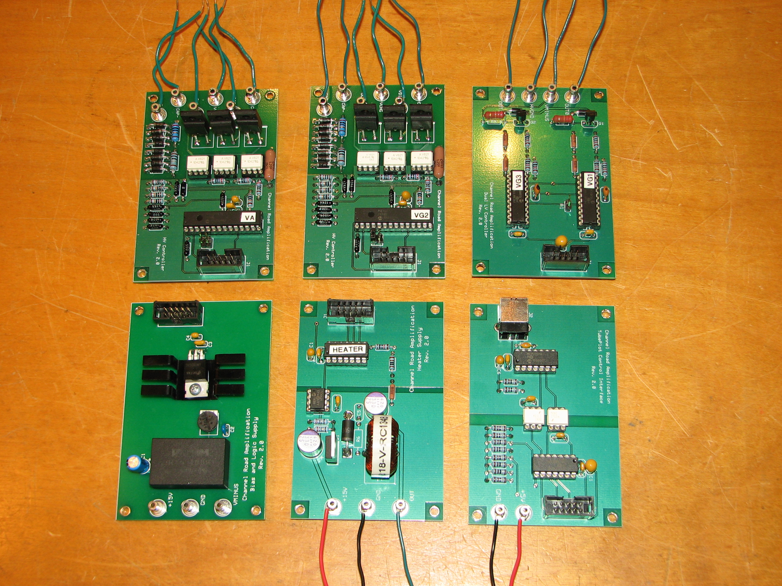
The tube analyzer is constructed on six small printed circuit boards (PCBs), each 3.8" × 2.5" in size. This worked out well for an initial implementation, though it might not make economic sense for a production version. My first motivation for using smaller PCBs was simply my lack of experience at laying out printed circuit boards. I found it much easier to lay out several small, simple PCBs than to lay out a larger, more complex board. Also, the modular nature of the design fit well with the smaller PCBs. Since the device has two identical high-voltage supplies and two identical low-voltage supplies, I could simply build two each of the high-voltage and low-voltage PCBs. (As it turned out, the low-voltage design was so simple that I easily fit both of them onto a single small PCB.) The photo at left shows the completed circuit boards. Clockwise from the upper left, they are: two high-voltage supplies; the dual low-voltage supply; the master controller (note the white opto-isolator chips); the heater supply (the first version, without current monitoring); and a PCB holding the +5V logic regulator and a DC-to-DC converter to power the B- bias supply.
I laid out the circuit boards using free CAD software from ExpressPCB and then ordered the boards through them. This was the reason for the size of the boards I used. ExpressPCB has a special deal for boards exactly that size at a reasonable price.
The modular construction paid off soon after I had finished the project. My original heater supply design had no provision for measuring the heater current. When I later decided to add that feature, it was easy to do by replacing the heater supply board with a new one.
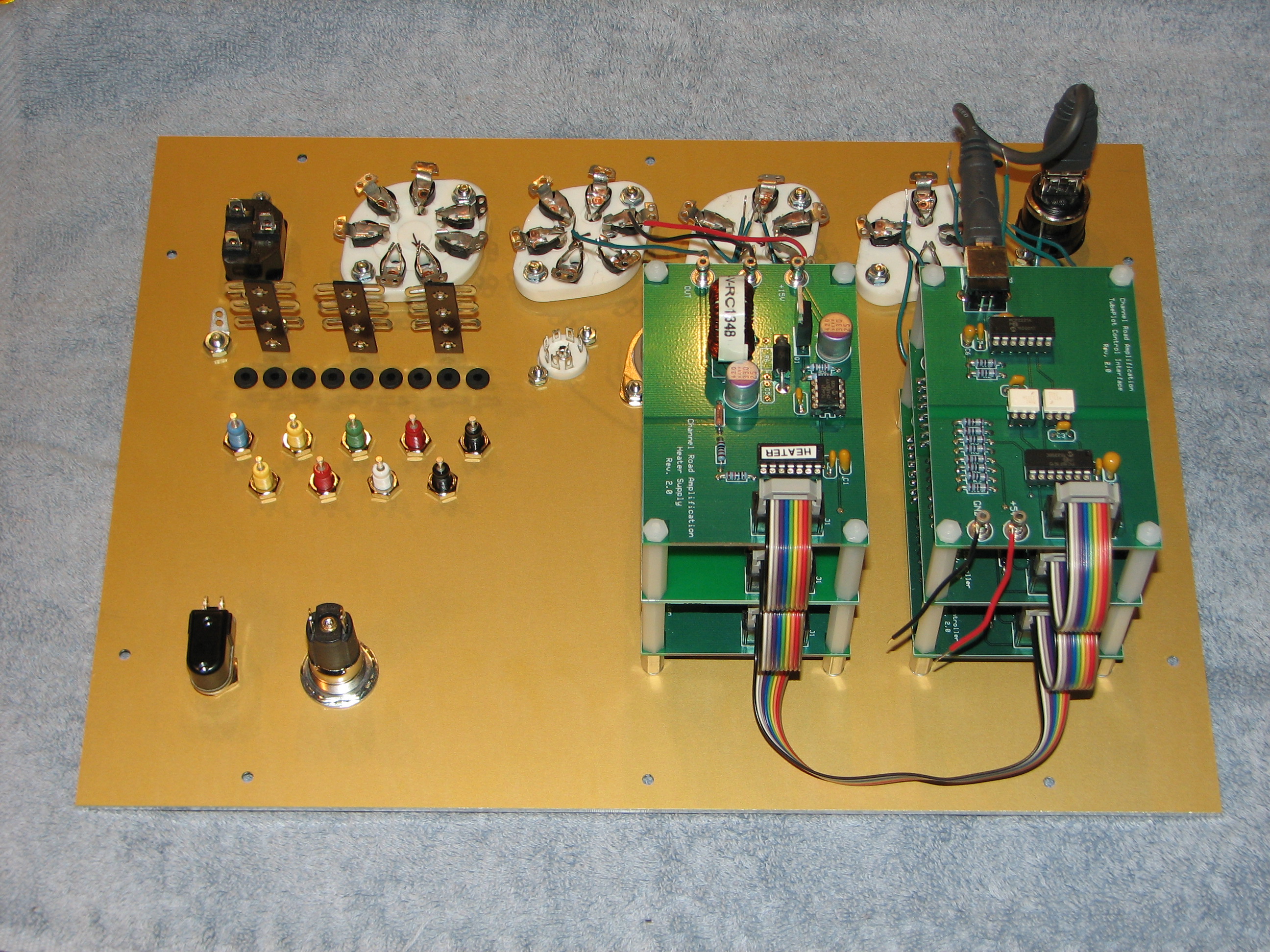
I assembled the completed circuit boards into two stacks mounted on the faceplate, as shown at right. The multicolored ribbon cable carries the logic power (+5V), ground, the I2C bus, and a few other signals used for synchronizing and coordinating the operation of the modules. Higher-voltage signals destined for the tube sockets terminate in turrets.
I ordered the metal faceplate from Front Panel Express. They are a bit pricey, but their faceplates always come out looking great. Their precision milling machines produce mounting holes of any desired shape and size, and every hole is exactly where it ought to be—much more accurate than I can make myself.
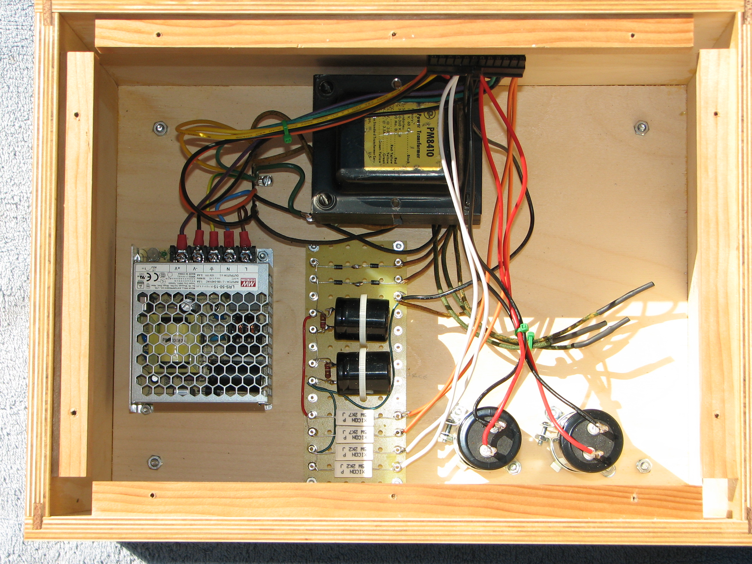
The faceplate forms the top face of a wood box that I built. I had never made a wood box before, so I got a lot of advice from a few friends who are experienced woodworkers. I built the box from ½-inch Baltic plywood, which turned out to be a great material for my first wood box. It is flat and stable, so it doesn't require a jointer-planer (a tool that I don't have, in any case). It is void-free, and the end grain looks good so it doesn't need to be covered up with veneer or miter joints or other more difficult techniques. A friend who is a retired cabinetmaker taught me how to make spline joints for holding the box together.
Some large electronic components are mounted in the bottom of the cabinet. These include a conventional 515-volt B+ supply for the high-voltage portion of the circuit, using a power transformer I had salvaged from an old piece of equipment. There are also a couple of very large capacitors for the two high-voltage supplies, and a commercial high-amperage 15-volt switching supply that powers the logic, the heater supply, and the bias supplies. These components connect to the circuitry on the faceplate via an ATX computer connector to facilitate removal of the faceplate.
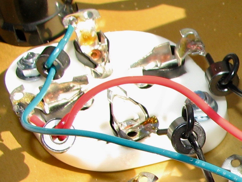
One challenge even with conventional tube testers is oscillation. By nature, tube testers tend to have long wires leading to their tube sockets, and the parasitic inductance and capacitance can easily cause certain kinds of tubes to oscillate. I ran into this problem when testing the breadboard version of the tube analyzer. Some tubes would produce plots that were random and nonsensical, with wild plot lines running every which way. I addressed the problem the same way tranditional tube testers have addressed it: by placing ferrite beads around the tube socket leads as close as possible to each socket. Ferrite beads are lossy at high frequencies, and they suppress oscillations by draining high-frequency energy from the system. Conventional tube testers often use ferrite beads on just a few key tube socket pins, based on their knowledge of the types of tubes that can be tested. For generality, I looped each and every tube socket lead through a ferrite bead right next to the socket. This was effective in eliminating the oscillation problem.
Copyright © 2018 John D. Polstra. All rights reserved.